

The scope, uses and sheer range of advanced materials seems to be growing every day. It is not just newly-invented materials that are breaking new ground; established materials like are being developed and enhanced with targeted qualities that are designed to improve sustainability. Lien Ngo, Innovate UK
A big challenge for exploiting novel materials is the scale up and manufacturing stage. Every once in a while, there is a call for a general pilot scale facility for materials, but this has always been a difficult proposition.
Too many for a single source
The world of materials is so varied and wide-ranging that the equipment needed for working with each type is very different, and gathering all the various specialist “pots and pans” required in one place would be impossible. For example, semiconductor materials require wafer fabrication facilities, lithography and very precise deposition of nanometer-thick layers of conductors and insulators. Metal alloys and novel powders for additive manufacturing often require extremely high temperatures; new, high tech steels require all the traditional steelmaking and rolling equipment as well as novel additions. New polymers and their synthesis and processing methods are a whole other ball game and have needs more similar to chemicals processing.
-
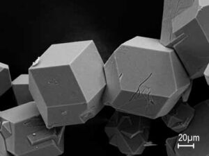
- Primary iron-rich intermetallic in Aluminium alloy.
-
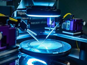
- Semiconductor materials require specialist wafer fabrication facilities
-
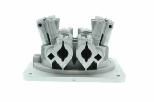
- Powders for the additive manufacture of products like this galvanometer block require extremely high temperatures.
This is the point, of course, where advanced materials and manufacturing meet, and it is why the High Value Manufacturing Catapult has seven centres, each having specialism in different kinds of materials and manufacturing. It would not only be too expensive, but impossible to have a pilot manufacturing facility covering every type of material.
Even the same broad class of materials can require very different equipment to make. For example, carbon fibre composites use very different equipment to metal matrix composites, both in the manufacturing and further processing into the final product. Manual lay-up, tooling and autoclaves are required for carbon fibre composites, while hot isostatic pressing is needed for metal matrix composites. In fact, even the same material can have radically different manufacturing processes. That ubiquitous wonder material, graphene, is a great example of this: nanoplatelets can be exfoliated, mechanically or chemically, from graphite sources; large area few layered graphenes can be “grown” in different ways; single layer graphene has to be grown on specialized substrates and then removed to be deposited into their final product-specific places. These all require vastly different equipment. When you get into the tonne (and sometimes even kilogram) scale, the equipment gets very expensive and the expertise more and more rare. When you take into account other 2D materials, arguably the true inheritors of graphene’s massive research push, the manufacturing challenges will be even more interesting.
Nanotechnology, like 2D materials, encompasses a broad and diverse set of materials covering the entire periodic table. In some of these sets of materials, there has certainly been good success in scaling up. For example, Promethean Particles was spun out from the University of Nottingham in 2007, with new techniques for synthesizing certain kinds of nanoparticles. I first met them a few years later on a mission to South Korea for small business working in printed electronics. They now have a production site producing nanoparticle dispersions at scale. These metals, oxides and nitrides are used in a variety of applications: electronics, catalysts, healthcare. Now, with investment from EU funding and Innovate UK, Promethean Particles can continuously produce these nanoparticles at a full production scale of 1000 tonnes annually.
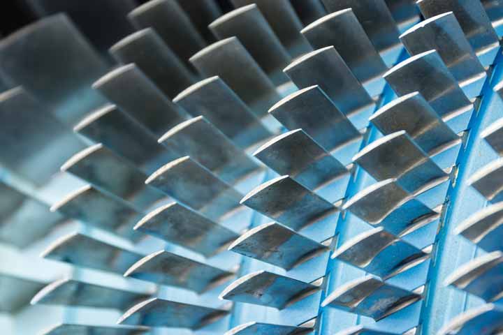
Aircraft engine manufacturers are increasingly seeking specialised materials for lightness and tailored properties.
One way in which new materials crosses with a manufacturing challenge is in the field of metamaterials. Metamaterials direct, block, guide, bend, amplify or otherwise modulate waves- generally waves of light or sound. (They are famous as the theoretical basis of an invisibility cloak, where the material bends light around the cloak so you are seeing what’s behind it.) Metamaterials are a triumph of structure over substance: their properties come from the arrangement and pattern of the shape- generally the feature size is smaller than the wavelengths the material is modulating- rather than the material itself. So acoustic metamaterials are patterned carefully, but they can be made from many materials which can be manufactured with that pattern. A metamaterial that acts as a lens for sound has been made by researchers at the University of Sussex partly using Lego bricks. In another example, Sonobex, a company spun out from Loughborough University, uses metamaterials to shield areas with heavy plant machinery, neutralizing noise but still allowing light in and air flow for cooling. The metamaterial panels are made from galvanized steel. Optical and electromagnetic metamaterials can be used to shield something from radar detection and as antenna for next generation li-fi communications.
Because the 3D patterning and structure are so important, and because it is vital to be able to tune the feature sizes and spacing to target the wavelengths you want, metamaterials may be one of those applications which can only reach its true potential with additive manufacturing methods, especially for acoustic and microwave applications. The complex structures needed are difficult to manufacture using conventional methods.
Graphene , the ‘wonder material’ is now being adopted by manufacturers and used at scale but making large-area single-layer graphene may be tipping from ruinously expensive to realistic.
GRAPHENE MANUFACTURING
Nineteen years after the Nobel Prize in Physics was awarded for the discovery of graphene, nearly all forms of it have moved into manufacturing at production scales and realistic prices. This was not true even a few years ago, but now graphene in nanoplatelets, as flakes or in dispersions, few layer flakes and even large area single layers are available and manufacturing is either already at large production scale or is obviously scalable. Two home-grown companies have had graphene products for some years now: Thomas Swan has a range of graphene nanoplatelet products and have scaled up to a 20 tonne per year production capacity; Versarien, with its Nanene product, sells few layer graphenes and stakes its reputation on quality, with a Verified Graphene Producer inspection from The Graphene Council.
In the technically tricky (read: ruinously expensive) manufacture of large area single layer graphene, which is what all those superlative performance numbers generally come from, I admit I was skeptical that anyone would ever make it at large enough scale and cheap enough for it to be realistically usable in any application bar some very esoteric, tiny volume uses. However, there is some evidence that modest-to-large scale production processes have been developed which are on target to reduce costs to 30-60USD/m2 of single-layer graphene made by chemical vapour deposition.